Electron backscatter diffraction (EBSD) is a scanning electron microscope–based microstructural-crystallographic characterization technique commonly used to study crystalline or polycrystalline materials.[1] EBSD is carried out in a scanning electron microscope (SEM) equipped with an EBSD detector comprising at least a phosphorescent screen, a compact lens and a low-light CCD camera. In this configuration, the SEM incident beam hits the tilted sample. As backscattered electrons leave the sample, they interact with the crystal’s periodic atomic lattice planes and diffract according to Bragg's law at various scattering angles before reaching the phosphor screen forming Kikuchi patterns (EBSPs).
The change and degradation in electron backscatter patterns (EBSPs) provide information about lattice distortion in the diffracting volume. Pattern degradation (i.e., diffuse quality) can be used to assess the level of plasticity. The EBSP zone axis position change can be used to measure the residual elastic stress and small lattice rotations. EBSD can also provide information about geometrically necessary dislocations (GND) density. However, the lattice distortion is measured relative to a reference pattern (EBSP0). The reference pattern choice affects the measurement precision; e.g., a reference pattern deformed in tension will directly reduce the HR-EBSD map tensile strain magnitude while indirectly influencing the other component magnitude and the strain’s spatial distribution. Furthermore, the choice of EBSP0 slightly affects the GND density distribution and magnitude.[2]
For electron backscattering diffraction microscopy, a flat polished crystalline specimen is usually placed inside a Scanning electron microscope (SEM) chamber, tilted ~70° from SEM original specimen positioning and 110° to the diffraction camera.[3] Tilting the sample elongates the interaction volume perpendicular to the tilt axis, allowing more electrons to leave the sample due to elastic scattering, providing better contrast.[4][5] The high-energy electron beam (typically 20 kV) is focused on a small volume and scatters at a spatial resolution of ~20 nm at the specimen surface.[6] The spatial resolution varies with angular width,[7] interaction volume,[8] nature of the material under study,[6] and in transmission Kikuchi diffraction with the specimen thickness;[9] thus, increasing the beam energy increases the interaction volume and decreases the spatial resolution.[10]
An electron backscatter diffraction pattern of monocrystalline silicon, taken at 20 kV with a field-emission electron source
The phosphor screen is located within the specimen chamber of the SEM at an angle of approximately 90° to the pole piece and is coupled to a compact lens which focuses the image from the phosphor screen onto the CCD camera and excite the phosphor causing it to fluoresce. In this configuration, as these backscattered electrons leave the sample, they interact with the crystal’s periodic atomic lattice planes and diffract according to Bragg's law at a range of scattering angles ().[11][12] The backscattered electrons form Kikuchi lines – having different intensities – on an electron-sensitive flat film/screen (commonly phosphor), gathered to form a Kikuchi band. These Kikuchi lines are the trace of hyperbola formed by the intersection of Kossel-cones with the plane of the phosphor screen. The width of a Kikuchi band is related to the scattering angles and, thus, lattice spacing ().[13][14] These Kikuchi lines and patterns were named after Seishi Kikuchi, who, together with Shoji Nishikawa [ja], was the first to notice this diffraction pattern in 1928 using TEM[15] which is similar in geometry to X-ray’s Kossel pattern.[16]
The systematically arranged Kikuchi bands, which have a range of intensity along their width, intersect around the centre of the regions of interest (ROI), describing the probed volume crystallography.[17] These bands and their intersections form what are known as Kikuchi patterns or electron backscatter patterns (EBSPs). To improve contrast, the patterns’ background is corrected by removing anisotropic/inelastic scattering using static background correction or dynamic background correction.[18]
Single crystal 4H SiC (gnomically projected) EBSP collected using (left) conventional, (centre) dynamic, and (right) combined background correctionFormation of Kossel cone which intersect with CCD screen to form EBSP which can be Bravais-Miller indexed
If the system geometry is well described, it is possible to relate the bands present in the diffraction pattern to the underlying crystal and orientation of the material within the electron interaction volume. Each band can be indexed individually by the Miller indices of the diffracting plane which formed it. In most materials, only three bands/planes which intersect are required to describe a unique solution to the crystal orientation (based upon their interplanar angles) and most commercial systems use look up tables with international crystal data bases to perform indexing. This crystal orientation relates the orientation of each sampled point to a reference crystal orientation.[3][19]
While this 'geometric' description related to the kinematic solution (using the Bragg condition) is very powerful and useful for orientation and texture analysis, it only describes the geometry of the crystalline lattice and ignores many physical processes involved within the diffracting material. To adequately describe finer features within the electron beam scattering pattern (EBSP), one must use a many beam dynamical model (e.g. the variation in band intensities in an experimental pattern does not fit the kinematic solution related to the structure factor).[20][21]
EBSD detectors
Experimentally EBSD is conducted using a SEM equipped with an EBSD detector containing at least a phosphor screen, compact lens and low light CCD camera. Commercially available EBSD systems typically come with one of two different CCD cameras: for fast measurements the CCD chip has a native resolution of 640×480 pixels; for slower, and more sensitive measurements, the CCD chip resolution can go up to 1600×1200 pixels.[12][6]
The biggest advantage of the high-resolution detectors is their higher sensitivity and therefore the information within each diffraction pattern can be analysed in more detail. For texture and orientation measurements, the diffraction patterns are binned in order to reduce their size and reduce computational times. Modern CCD-based EBSD systems can index patterns at up to 1800 patterns/second. This enables very rapid and rich microstructural maps to be generated.[13][22]
Sample preparation
Ideally, the sample should be vacuum-stable and mounted using a conductive compound (e.g. Cu and SiO2 filled epoxy thermoset) because it minimises image drift and the intensity blooming caused by the electron beam charging. Due to EBSPs quality being highly sensitive to the surface preparation, the sample should be ground using SiC papers from 240 down to 4000 grit, and polished using diamond paste (from 9 to 1 µm) then in 50 nm colloidal silica for 2 hours (50rpm speed and 5N force) to produce a flat surface without preparation-induced artefacts and also to maintain consistency – for comparison – between samples. Afterwards, the sample should be cleaned for 20 minutes in Ultrasonic cleaning bath using ethanol, then rinsed with deionised water, before eventually being dried with a hot air blower. This is followed by ion polishing, for final surface preparation, using 7.5 keV dual beam energy for 15 min, with the gun’s angle of 8°.[23][24][25]
Inside the scanning electron microscope (SEM), the size of the measurement area determines local resolution and measurement time.[26] For high-quality EBSPs, it is recommended[27][28][29][30] to use 15 nA current, 20 keV beam energy, 18mm working distance, long exposure times and minimal pattern binning. The EBSD phosphor screen should be also at 18mm working distance with at least 800*600 resolution, 180 milli-seconds exposure time per pattern, 2*2 pattern binning, and a map’s step size less than 0.5µm.[31][32]
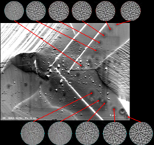
Pattern degradation due to carbon deposition in a highly magnified location after 3hr EBSPs acquisition around a deformation twin in the ferrite phase of duplex stainless steel.[32]
The effect of carbon deposition on the quality of the patterns, which is caused by the electron-beam-induced decomposition of gaseous hydrocarbons during slow EBSPs acquisition.[33] Carbon depositions degrade the quality of EBSPs inside the probed area compared to the EBSPs outside the acquisition window. The gradient of pattern degradation increases moving inside the probed zone with an apparent accumulation of deposited carbon. The black spots from the beam instant-induced carbon deposition also highlight the immediate deposition even if agglomeration did not happen.[34][35]
Electron-matter interaction volume and various types of signal generated
The depth resolution of EBSD is widely accepted to vary between 10 to 40 nm, decreasing with the material atomic number.[36] Nevertheless, using a differently thick transparent amorphous layer of Chromium coating a mono-Silicon crystal, experimental measurements indicated that the depth resolution could be as shallow as 2 nm. This was determined by Si pattern quality deteriorating by ~50% when using a FEG-SEM with 15 kV beam conditions and 15 mm working distance between the beam and sample and 65 mm between the sample and the detector and without considering the channelling effect.[37] However, using a similar experimental approach, different results were reported, e.g., Isabell and David[38] concluded that depth resolution could extend to 1 µm due to inelastic scattering (including tangential smearing and channelling effect).
These experiments are highly cumbersome due to the need for precise and well-calibrated equipment, with the results open to interpretation.[39] This is partially because there is no agreement about the definition of depth resolution. For example, definitions in the literature include those where the depth is where ~92% of the signal is generated,[40][41] or defined by pattern quality,[37] or are as ambiguous as “where useful information is obtained”.[42] The reported values in Table 9‑5 either do not mention a definition or do not have a rationale for the definition of depth resolution. In addition, most of these experiments do not provide information on the beam size, tilt angle, beam-to-sample and sample-to-detector working distance, and – sometimes – even the beam energy. These are critical parameters for determining (or simulating) the depth resolution of the patterns as the interaction volume, which decreases with the sample atomic number or density, increases with beam energy and size.[38] The beam current is generally not considered to affect the depth resolution in experiments or simulations. However, it affects the beam spot size and pattern signal-to-noise (S/N) ratio,[43][44][45] affecting the depth resolution and the details in the pattern.
Illustrate of the interaction of an electron beam with a sample. Where K,L,M are the electron shells. N is the sample nucleus. Gamma is a characteristic photon emitted by the ejection of SE (Secondary Electron). BSE is a Back-Scattered Electron. Electrons
Using Monte Carlo (MC) simulations is also an alternative approach to quantifying the depth resolution for EBSPs formation which can be estimated using Bloch wave theory, where backscattered primary electrons - after interacting with the crystal lattice - exit the surface carrying information about the crystallinity of volume interacting with the electrons. The backscattered electrons (BSE) energy distribution depends on the material’s characteristics and the beam conditions.[46] This BSE wave field is also affected by the thermal diffuse scattering process that causes incoherent and inelastic (energy loss) scattering – after the Bragg diffraction events – which does not, yet, have a complete physical description that can be related to mechanisms that constitute EBSP depth resolution.[47][21]
Most importantly, conclusions drawn from both experiments and simulations assume the surface is pristine with homogeneity of the depth resolution, neither of which is valid for a deformed sample.[37]
Orientation and phase mapping
Pattern indexing
Overview of EBSD indexing procedure showing pattern capture through to determination of crystal orientation[22]
Often, the first step in the EBSD process after pattern collection is indexing. This allows for the identification of the crystal orientation at the single volume of the sample from where the pattern was collected.[48][49] With EBSD software, pattern bands are typically detected via a mathematical routine using a modified Hough transform, in which every pixel in Hough space denotes a unique line/band in the EBSP. The Hough transform is used to enable band detection, which is difficult to locate by computer in the original EBSP. Once the band locations have been detected it is possible to relate these locations to the underlying crystal orientation, as angles between bands represent angles between lattice planes. Thus when the position/angles between three bands are known an orientation solution can be determined. In highly symmetric materials, typically more than three bands are used to obtain and verify the orientation measurement. There are two leading methods of the indexing performed by most commercial EBSD software: triplet voting;[50][51] minimising the 'fit' between the experimental pattern and a computationally determined orientation,[52][53] and or/and neighbour pattern averaging and re-indexing NPAR[54]) to give a unique solution to the single crystal orientation that is related to the other crystal orientations within the field-of-view.[55][56]
Triplet voting involves identifying multiple 'triplets' associated with different solutions to the crystal orientation; each crystal orientation determined from each triplet receives one vote. Should four bands identify the same crystal orientation then four (four choose three) votes will be cast for that particular solution. Thus the candidate orientation with the highest number of votes will be the most likely solution to the underlying crystal orientation present. The ratio of votes for the solution chosen as compared to the total number of votes describes the confidence in the underlying solution. Care must be taken in interpreting this 'confidence index' as some pseudo-symmetric orientations may result in low confidence for one candidate solution vs. another.[57][58][59]
Minimising the fit involves starting with all possible orientations for a triplet. More bands are included that reduces the number of candidate orientations. As the number of bands increases, the number of possible orientations converge ultimately to one solution. The 'fit' between the measured orientation and the captured pattern can be determined.[56]
Pattern centre
In order to relate the orientation of a crystal, much like in X-ray diffraction, the geometry of the system must be known. In particular the pattern centre, which describes both the distance of the interaction volume to the detector and the location of the nearest point between the phosphor and the sample on the phosphor screen. Early work used a single crystal of known orientation being inserted into the SEM chamber and a particular feature of the EBSP was known to correspond to the pattern centre. Later developments involved exploiting various geometric relationships between the generation of an EBSP and the chamber geometry (shadow casting and phosphor movement).[60][56]
Unfortunately, each of these methods are cumbersome and can be prone to some systematic errors for a general operator. Typically they can not be easily used in modern SEMs with multiple designated uses. Thus, most commercial EBSD systems use the indexing algorithm combined with an iterative movement of both crystal orientation and suggested pattern centre location. Minimising the fit between bands located within experimental patterns and those in look up tables tends to converge on the pattern centre location to an accuracy of ~0.5–1% of the pattern width.[22][6]
Recent development of AstroEBSD[61] and PCGlobal,[62] open-source MATLAB codes, increased the precision of determining the pattern centre (PC) and – consequently – elastic strains[63] by using a pattern matching approach[64] which simulates the pattern using EMSoft.[65]
EBSD mapping
EBSD orientation (indexed) map about ferrous lath martensite with high angle (>10°) boundaries.
EBSD can be used to find the crystal orientation of the material located within the incident electron beam's interaction volume.[66] Thus by scanning the electron beam in a prescribed fashion (typically in a square or hexagonal grid, correcting for the image foreshortening due to the sample tilt) results in many rich microstructural maps.[67][68] These maps can spatially describe the crystal orientation of the material being interrogated and can be used to examine microtexture and sample morphology. Some of these maps describe grain orientation, grain boundary, diffraction pattern (image) quality. Various statistical tools can be used to measure the average misorientation, grain size, and crystallographic texture. From this dataset, numerous maps, charts and plots can be generated.[69][70][71]
However, microscope alignments, image shifts, scan distortion that increases with decreasing magnification, ill-prepared contaminated and rough specimen surface, changes in material, boundary indexing failure and detector quality can lead to uncertainties in determining the crystal orientation.[72][72] Fundamentally, the EBSD pattern’s signal-to-noise ratio is material dependent and decreases with high acquisition speeds and beam currents, which directly affects the angular resolution of the measurements.[72][72]
Integrated EBSD/EDS mapping
When simultaneous Energy-dispersive X-ray spectroscopy (EDS)/EBSD collection can be achieved, the capabilities of both techniques can be enhanced.[73] There are applications where sample chemistry or phase cannot be differentiated via EDS alone because of similar composition; and structure cannot be solved with EBSD alone because of ambiguous structure solutions.[74][75] To accomplish integrated mapping, the analysis area is scanned and at each point Hough peaks and EDS region-of-interest counts are stored. Positions of phases are determined in X-ray maps and measured EDS intensities are given in charts for each element. For each phase the chemical intensity ranges are set to select the grains.[76] All patterns are then re-indexed off-line. The recorded chemistry determines which phase / crystal structure file is used for indexing of each point. Each pattern is indexed by only one phase and maps displaying clearly distinguished phases are generated. The interaction volumes for EDS and EBSD are significantly different (on the order of micrometers compared to tens of nanometers) and the shape of these volumes using a highly tilted sample may have implications on algorithms for phase discrimination.[19][77]
Full-field displacements, elastic strains, and the geometrically necessary dislocations (GND) density provide quantifiable information about the the material’s elastic and plastic behaviour at the microscale. Measuring strain at the microscale requires careful consideration of other key details besides the change in length/shape (e.g., local texture, individual grain orientations). These micro-scale features can be measured using different techniques, e.g., hole drilling, monochromatic or polychromaticenergy-dispersiveX-ray diffraction (XRD) or neutron diffraction (ND). However, the electron backscattering diffraction (EBSD) technique provides an impressive combination of sensitivity, spatial resolution and ease of use compared to other techniques.[71][84][85]
Earlier trials
The change and degradation in electron backscatter patterns (EBSPs) provide information about the diffracting volume. Pattern degradation (i.e., diffuse quality) can be used to assess the level of plasticity through the pattern/image quality (IQ),[86] where IQ is calculated from the sum of the peaks detected when using the conventional Hough transform. Wilkinson[87] first used the changes in high-order Kikuchi line positions to determine the elastic strains, albeit with low precision[note 1] (0.3% to 1%); however, this approach cannot be used for characterising residual elastic strain in metals as the elastic strain at the yield point is usually around 0.2%. Measuring strain by tracking the change in the higher-order Kikuchi lines is practical when the strain is small, as the band position is sensitive to changes in lattice parameters.[88] In the early 1990s, Troost et al.[89] and Wilkinson et al.[90][91] used pattern degradation and change in the zone axis position to measure the residual elastic strains and small lattice rotations with a 0.02% precision.[2]
High resolution electron backscatter diffraction (HR-EBSD)
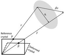
Schematic shifting between a reference and deformed crystals in the EBSP pattern projected in the phosphor screen[32]
Cross-correlation-based, high angular resolution electron backscatter diffraction (HR-EBSD) – introduced by Wilkinson et al.[92][93] – is a scanning electron microscopy (SEM) -based technique to map relative elastic strains and rotations, and estimate the geometrically necessary dislocation (GND) density in crystalline materials. HR-EBSD method uses image cross-correlation to measure pattern shifts between regions of interest (ROI) in different electron backscatter diffraction patterns (EBSPs) with sub-pixel precision. As a result, the relative lattice distortion between two points in a crystal can be calculated using pattern shifts from at least four non-collinear ROI. In practice, pattern shifts are measured in more than 20 ROI per EBSP to find a best-fit solution to the deformation gradient tensor, representing the relative lattice distortion.[note 2][95][93]
The displacement gradient tensor () (or local lattice distortion) relates the measured geometrical shifts from in the pattern between the collected point () and associate (non-coplanar) vector (), and reference point () pattern and associate vector (). Thus, the (pattern shift) vector () can be written as in equations below, where and are the direction and displacement in th direction, respectively.[96]
The shifts are measured in the phosphor (detector) plane (), and the relationship is simplified; thus, eight out of the nine displacement gradient tensor components can be calculated by measuring the shift ( and ) at four distinct, widely spaced regions on the EBSP.[93][97] This shift is then corrected to the sample frame (flipped around Y-axis) because EBSP is recorded on the phosphor screen and is inverted as in a mirror. Then corrected around the X-axis by 24° (i.e., 20° sample tilt plus ≈4° camera tilt and assuming no angular effect from the beam movement[22]). Using infinitesimal strain theory, the deformation gradient is then split into elastic strain (symmetric part, where ), and lattice rotations (asymmetric part, where ), .[93]
These measurements do not provide information about the volumetric/hydrostatic strain tensors. By imposing a boundary condition that the stress normal to the surface () is zero (i.e., traction-free surface[98]), and using Hooke’s law with anisotropic elastic stiffness constants, the missing ninth degree of freedom can be estimated in this constrained minimization problem by using a nonlinear solver.[93]
Where is the crystal anisotropic stiffness tensor. These two equations are solved to re-calculate the refined elastic deviatoric strain () including the missing ninth (spherical) strain tensor. An alternative approach that considers the full can be found in.[98]
Finally, the stress and strain tensors are linked using the crystal anisotropic stiffness tensor (), and by using Einstein summation convention with symmetry of stress tensors ().[95]
The quality of the produced data can be assessed by taking the geometric mean of all the ROI’s correlation intensity/peaks, and a value lower than 0.25 should indicate problems with the EBSPs quality.[97] Furthermore, the geometrically necessary dislocation (GND) density can be estimated from the HR-EBSD measured lattice rotations by relating the rotation axis and angle between neighbour map points to the dislocation types and densities in a material using Nye’s tensor.[31][99][100]
Precision and development
The HR-EBSD method was shown[93][101] to achieve a precision of ±10–4 in components of the displacement gradient tensors (i.e., strain and rotation in radians) by measuring the shifts at a pattern image resolution of ±0.05 pixels. Still, it was limited to small strains and rotations (>1.5°). Britton and Wilkinson[95] raised the rotation limit to ≈11° by using a re-mapping technique[102] that recalculated the strain after transforming the patterns with a rotation matrix () calculated from the 1st cross-correlation iteration.
(a) Secondary electron (SE) image for the indentation on the (001) mono crystal. (b) HR-EBSD stress and rotation components, and geometrical necessary dislocations density (. EBSP0 is highlighted with a star in [103]
However, further lattice rotation, typically caused by severe plastic deformation, will cause errors in the elastic strain calculations. Ruggles et al.[104] demonstrated an improved HR-EBSD precision, even at 12° of lattice rotation, using the inverse compositional Gauss–Newton-based (ICGN) method instead of cross-correlation. Vermeij and Hoefnagels[105] also established a method that achieves a precision of ±10–5 in the displacement gradient components using a full-field integrated digital image correlation (IDIC) framework instead of dividing the EBSPs into small ROIs. Patterns in IDIC are distortion-corrected to negate the need for re-mapping up to ≈14°.[106][107] Below comparison of conventional Hough transform EBSD and HR-EBSD[93][108]
Conventional EBSD
HR-EBSD
Absolute Orientation
2°
N/A
Misorientation
0.1° to 0.5°
0.006° (1 x 10⁻⁴ rad)
GND @ 1 µm step
In lines/m2 (b = 0.3 nm)
> 3 x 10¹³
> 3 x 10¹¹
Relative Residual Strain
N/A
Deviatoric elastic strain 1 x 10⁻⁴
Example Tasks
Texture, Microstructure, etc.
Deformation
However, these measurements do not provide information about the volumetric/hydrostatic strains,[95][93] because there is no change in the plane or angles of the lattice planes (crystallographic directions) but only changes in the position/width of the Kikuchi bands (and their energetic correspondence).[109][110]
The reference pattern problem
Nonetheless, in HR-EBSD analysis, the lattice distortion field is still calculated relative to a reference pattern or point (EBSP0) per grain in the map, and is dependent on the lattice distortion at the point. The lattice distortion field in each grain is measured with respect to this point; therefore, the absolute lattice distortion at the reference point (relative to the unstrained crystal) is excluded from the HR-EBSD elastic strain and rotation maps.[108][111] This ‘reference pattern problem’ is similar to the ‘d0 problem’ in X-ray diffraction,[13][112] and affects the nominal magnitude of HR-EBSD stress fields. However, selecting the reference pattern (EBSP0) plays a key role, as severely deformed EBSP0 adds phantom lattice distortions to the map values, thus, decreasing the measurement precision.[108]
Linear correlation coefficients between the local conditions at the EBSP0 point and the averaged conditions at the grain for the ferrite (Fe-α) and austenite (Fe-γ) phase of age-hardened DSS, and Silicon (Si). The analysis considers the average deformation gradient tensor determinant (), maximum in-plane principal strain (), rotation magnitude (), correlation peak height (PH), mean angular error (MAE) and GND density.[2]
The local lattice distortion at the EBSP0 influences the resultant HR-EBSD map, e.g., a reference pattern deformed in tension will directly reduce the HR-EBSD map tensile strain magnitude while indirectly influencing the other component magnitude and the strain’s spatial distribution. Furthermore, the choice of EBSP0 slightly affects the GND density distribution and magnitude, and choosing a reference pattern with a higher GND density reduces the cross-correlation quality, changes the spatial distribution and induces more errors than choosing a reference pattern with high lattice distortion. Additionally, there is no apparent connection between EBSP0’s IQ and EBSP0's local lattice distortion.[2]
The use of simulated reference patterns for absolute strain measurement is still an active area of research[20][113][114][115][116][117][118][119] and scrutiny[108][120][121][122][123][124][125] as difficulties arise from a variation of inelastic electron scattering with depth which limits the accuracy of dynamical diffraction simulation models, and imprecise determination of the pattern centre which leads to phantom strain components which cancel out when using experimentally acquired reference patterns. Other methods assumed that absolute strain at EBSP0 can be determined using crystal plasticity finite-element (CPFE) simulations, which then can be then combined with the HR-EBSD data (e.g., using linear ‘top-up’ method[126][127] or displacement integration[128]) to calculate the absolute lattice distortions.
In addition, GND density estimation is nominally insensitive to (or negligibly dependent upon[129][130]) EBSP0 choice, as only neighbour point-to-point differences in the lattice rotation maps are used for GND density calculation.[131][132] However, this assumes that the absolute lattice distortion of EBSP0 only changes the relative lattice rotation map components by a constant value which vanishes during derivative operations, i.e., lattice distortion distribution is insensitive to EBSP0 choice.[111][2]
Selecting a reference pattern
Existing criteria for EBSP0 selection can be one or a mixture of:
Selecting from points with low GND density or low Kernel average misorientation (KAM)[133] based on the Hough measured local grain misorientations;
Selecting from points with high image quality (IQ), which may have a low defect density within its electron interaction volume, and is therefore assumed to be a low-strained region of a polycrystalline material.[134][135] However, IQ does not carry a clear physical meaning,[136] and the magnitudes of the measured relative lattice distortion are insensitive to the IQ of EBSP0;[111][2]
EBSP0 can also be manually selected to be far from potential stress concentrations such as grain boundaries, inclusions, or cracks using subjective criteria;[111]
Selecting an EBSP0 after examining the empirical relationship between the cross-correlation parameter and angular error, which was used in an iterative algorithm to identify the optimal reference pattern that maximises the precision of HR-EBSD.[2]
These criteria assume these parameters can indicate the strain conditions at the reference point, which can produce an accurate measurements of up to 3.2 x 10⁻⁴ elastic strain.[101] However, experimental measurements point to the inaccuracy of HR-EBSD in determining the out-of-plane shear strain components distribution and magnitude.[137]
Notes
^Throughout the Wikipedia page, the terms ‘error’, and ‘precision’ were used as defined in the International Bureau of Weights and Measures (BIPM) guide to measurement uncertainty (GUM). The true value in any measurement is in practice unknowable, therefore treat ‘error’, ‘accuracy’, and ‘uncertainty’ as synonymous, and ‘true value’ and ‘best guess’ as synonymous. Precision is the variance (or standard deviation) between all estimated quantities. Bias is the difference between the average of measured values and an independently measured ‘best guess’. Accuracy is then the combination of bias and precision.[2]
^Strain, distortion, and deformation can refer to several quantities in different fields. Therefore, we define our use of these terms (in italics) as follows. A mechanically loaded object changes shape in response to applied load; when measured in a mechanical test frame, it is called (total) engineering strain. Plastic strain is called the shape change that persists after the macroscopic load is removed. On the microscale, plastic deformation in most crystalline materials is accommodated by dislocation glide and deformation twinning. However, dislocations are also generated in a material as plastic deformation progresses, and dislocations with similar crystallographic character and sign that end up near each other in a material (e.g., lined up at a slip band) can be characterised as geometrically necessary dislocations (GNDs). Increasing plastic strain in a polycrystal also elastically distorts the crystal lattice to accommodate crystal defects (e.g., dislocation cores), groups of defects (e.g., dislocation cell walls), and maintains compatibility at polycrystal boundaries. This lattice distortion can be expressed as a deformation gradient tensor, which can be decomposed into elastic strain (symmetric) and lattice rotation (antisymmetric) components.[94] In this Wikipedia article, we use the term lattice distortion as a general term to refer to elastic distortion components derived from the deformation gradient, elastic strain, and lattice rotation tensors.
^Goldstein, Joseph I.; Newbury, Dale E.; Michael, Joseph R.; Ritchie, Nicholas W. M.; Scott, John Henry J.; Joy, David C. (2018), "Backscattered Electrons", Scanning Electron Microscopy and X-Ray Microanalysis, New York, NY: Springer New York, pp. 15–28, doi:10.1007/978-1-4939-6676-9_2, ISBN978-1-4939-6674-5, archived from the original on 3 March 2023, retrieved 2 March 2023
^ abEades, Alwyn; Deal, Andrew; Bhattacharyya, Abhishek; Hooghan, Tejpal (2009), Schwartz, Adam J.; Kumar, Mukul; Adams, Brent L.; Field, David P. (eds.), "Energy Filtering in EBSD", Electron Backscatter Diffraction in Materials Science, Boston, MA: Springer US, pp. 53–63, doi:10.1007/978-0-387-88136-2_4, ISBN978-0-387-88136-2, archived from the original on 3 March 2023, retrieved 2 March 2023
^Goldstein, Joseph I.; Newbury, Dale E.; Michael, Joseph R.; Ritchie, Nicholas W. M.; Scott, John Henry J.; Joy, David C. (2018), Goldstein, Joseph I.; Newbury, Dale E.; Michael, Joseph R.; Ritchie, Nicholas W.M. (eds.), "The Visibility of Features in SEM Images", Scanning Electron Microscopy and X-Ray Microanalysis, New York, NY: Springer, pp. 123–131, doi:10.1007/978-1-4939-6676-9_8, ISBN978-1-4939-6676-9, archived from the original on 3 March 2023, retrieved 3 March 2023
^Koko, Abdalrhaman; Marrow, James; Elmukashfi, Elsiddig (12 June 2022). "A Computational Method for the Determination of the Elastic Displacement Field using Measured Elastic Deformation Field". arXiv:2107.10330 [cond-mat.mtrl-sci].
^Koko, Abdalrhaman; Marrow, James; Elmukashfi, Elsiddig (12 June 2022). "A Computational Method for the Determination of the Elastic Displacement Field using Measured Elastic Deformation Field". arXiv:2107.10330 [cond-mat.mtrl-sci].
Schwartz, Adam J.; Kumar, Mukul; Adams, Brent L.; Field, David P., eds. (2009). Electron Backscatter Diffraction in Materials Science (2nd ed.). New York, NY: Springer New York, NY (published 12 August 2009). doi:10.1007/978-0-387-88136-2. ISBN978-0-387-88135-5.
Ruggles, T. J.; Bomarito, G. F.; Qiu, R. L.; Hochhalter, J. D. (1 December 2018). "OpenXY (HR-EBSD)". GitHub.((cite web)): CS1 maint: multiple names: authors list (link)